qu\'est-ce que tu cherches?
Recherches populaires
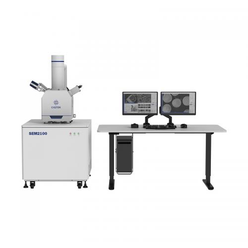
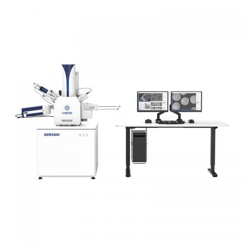
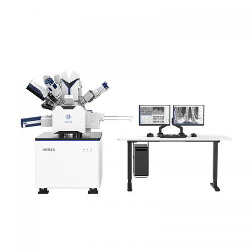
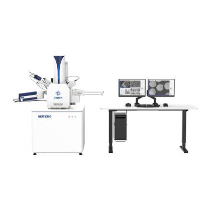
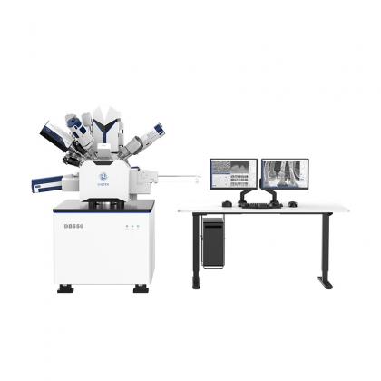
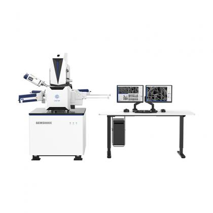
- Fournisseur mondial de fabricant et fournisseur mondial de microscope électronique à balayage à émission de champ
- Détecteurs SEM EDX, EDS, EBSD, BSE, CL, STEM
- Magnétomètre à balayage NV Microscope à force atomique à diamant quantique Applications QDAFM
- fabricant de microscope central à balayage NV ciqtek
- Fournisseur mondial de magnétométrie NV à balayage
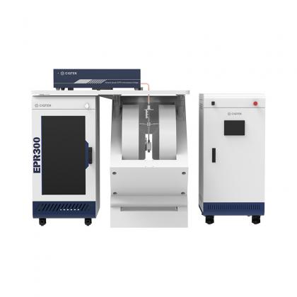
- Fournisseur mondial de spectroscopie de résonance paramagnétique électronique à impulsion en bande X
- Spectroscopie de résonance paramagnétique électronique meilleur prix
- Spectroscopie EPR en bande X avec cryostat
- Spectroscopie de résonance paramagnétique électronique en bande W, meilleur prix
- Spectroscopie de résonance de spin électronique en bande W, meilleur prix